My Store
Custom GaAs Substrates & Wafers for RF & Optoelectronics
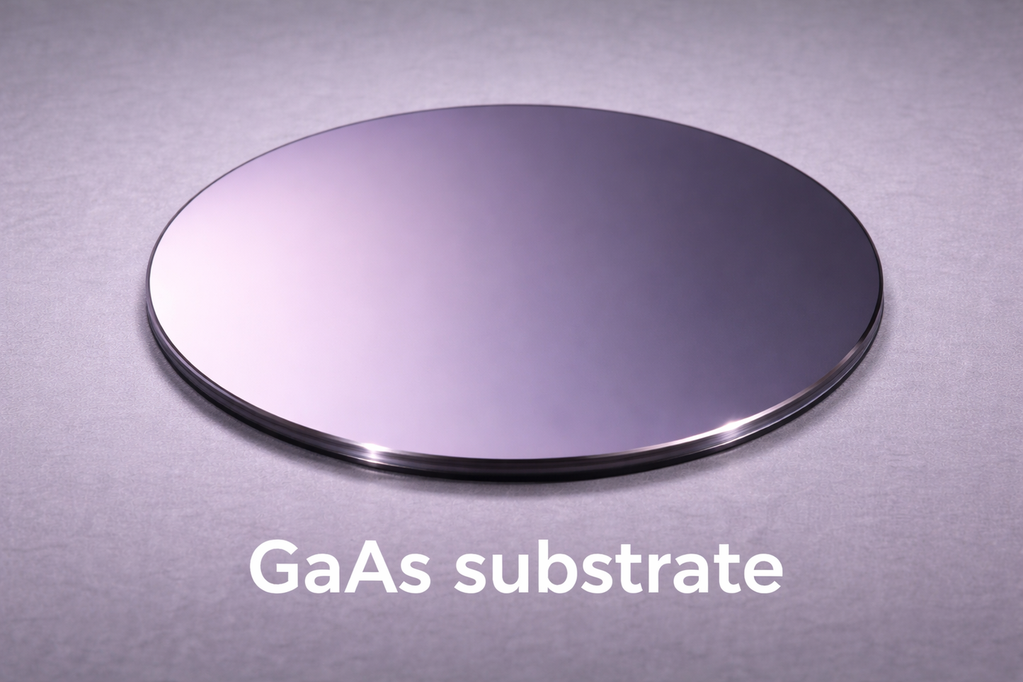
Custom GaAs Substrates & Wafers for RF & Optoelectronics
Couldn't load pickup availability
GaAs (Gallium Arsenide) is a high-performance III–V compound semiconductor widely used in RF and microwave devices, optoelectronics, high-speed electronics, and infrared photonics. With a direct bandgap of approximately 1.42 eV and very high electron mobility, GaAs enables devices that outperform silicon in high-frequency and low-noise applications.
Compared with silicon, GaAs offers higher electron mobility, direct bandgap emission, lower noise characteristics, and superior performance at microwave and millimeter-wave frequencies. These properties make GaAs the material of choice for HEMTs, MMICs, laser diodes, photodetectors, and high-speed ICs.
GaAs substrates provide excellent lattice matching for homoepitaxial and heteroepitaxial growth of III–V materials such as AlGaAs and InGaAs. Their well-controlled crystal orientation and surface quality are critical for MBE and MOCVD epitaxial growth.
Our GaAs wafers are supplied with tight control of orientation, thickness uniformity, surface flatness, and defect density. Optical- and epi-ready polishing is available to support both research laboratories and commercial device manufacturing.
Key Features
- Direct bandgap semiconductor (Eg ≈ 1.42 eV)
- Very high electron mobility
- Excellent RF and microwave performance
- Low noise characteristics
- Compatible with MBE and MOCVD epitaxy
- Available in semi-insulating and doped types
Typical Applications
- RF and microwave MMICs
- HEMT and MESFET devices
- Laser diodes and LEDs
- Infrared photodetectors
- High-speed and low-noise electronics
- III–V semiconductor research and epitaxy
Typical Properties
- Material: Gallium Arsenide (GaAs)
- Crystal Structure: Zinc blende
- Bandgap: ~1.42 eV (direct)
- Electron Mobility: ~8500 cm²/V·s
- Orientation: (100), (111) available
- Conductivity: Semi-insulating, n-type, p-type
Frequently Asked Questions — GaAs Substrate / Wafer
Share