My Store
Ga2O3 Substrates & Wafers for Ultra-Wide Bandgap Devices
Ga2O3 Substrates & Wafers for Ultra-Wide Bandgap Devices
Couldn't load pickup availability
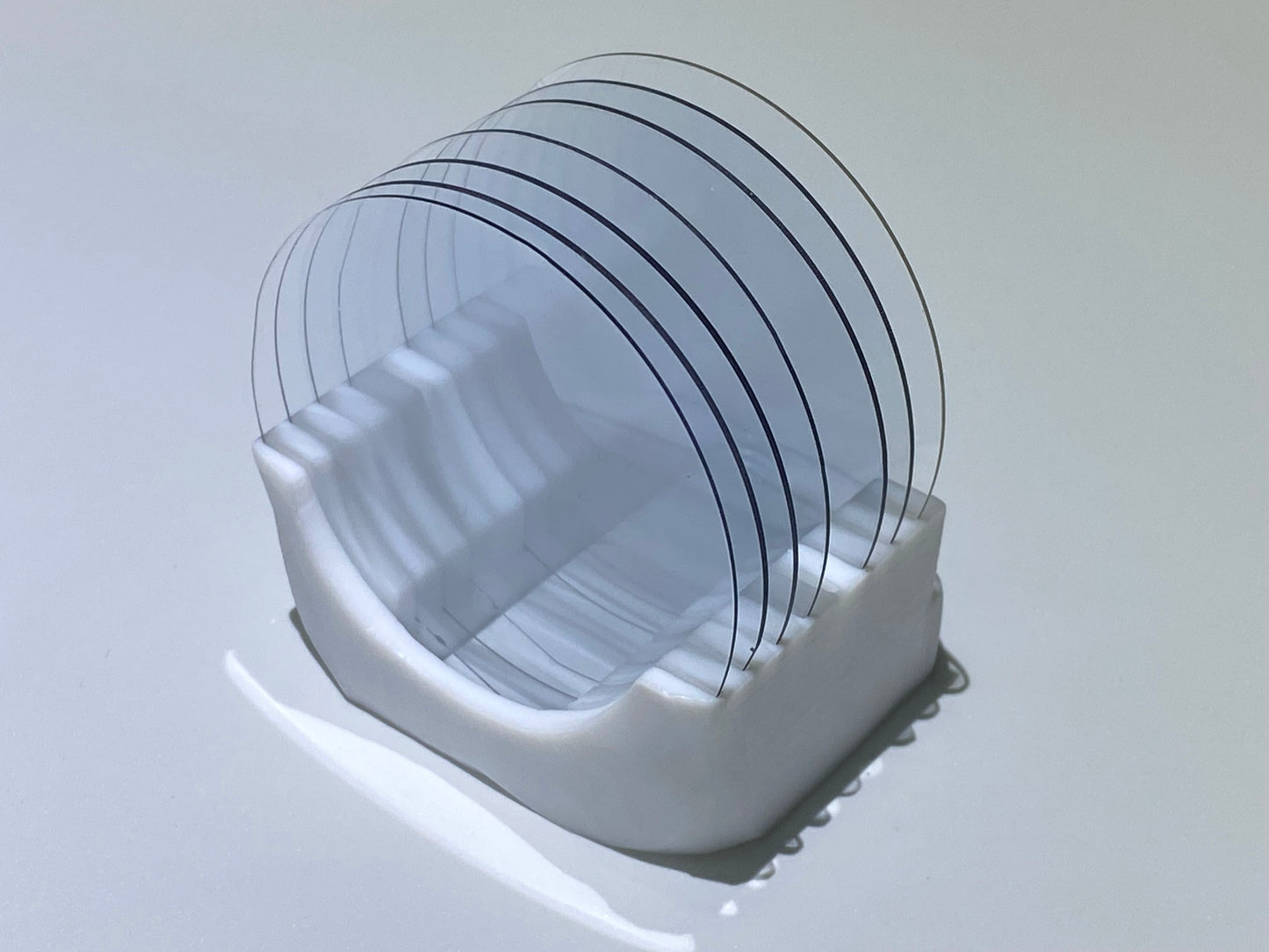
Ga₂O₃ (Gallium Oxide) substrates/wafers are cutting-edge materials enabling next-generation power semiconductor and deep-ultraviolet (DUV) applications. With an ultra-wide bandgap of approximately 4.9 eV, Ga₂O₃ offers exceptional breakdown voltage, thermal stability, and energy efficiency—outperforming traditional semiconductor materials.
Engineered for superior crystal quality and low defect density, these wafers are ideal for developing high-efficiency power devices, solar-blind photodetectors, and advanced RF components. Multiple crystal orientations and customizable specifications are available to meet both research and commercial production requirements.
Key Properties:
- 5mm x 5mm x 0.8mm
- Orientation: (100) (001), (010), (-201)
- Dopant Options: Sn (>1×10¹⁸ cm⁻³), Fe (>1×10¹⁰ Ω·cm)
- Surface Roughness (Ra): <0.5 nm
- Available Sizes: Standard and large formats
Contact us ( provide applications or exacatly requirements such as polished sides(single or double), orientation). Thank you
Frequently Asked Questions — Ga₂O₃ Substrates / Wafers
What is Ga₂O₃ and why is it important?
How does Ga₂O₃ compare with SiC and GaN?
What crystal orientation do you provide?
What dopant options are available?
What surface quality and roughness can be achieved?
What wafer sizes and thicknesses are available?
What applications commonly use Ga₂O₃ substrates?
Are Ga₂O₃ wafers suitable for research and commercial development?
📘 Related Knowledge
Share