My Store
CVD Diamond Wafers & Substrates for Power & RF Devices
CVD Diamond Wafers & Substrates for Power & RF Devices
Couldn't load pickup availability
Multi sizes and deposited wafers are also available. Please contact us for further information.
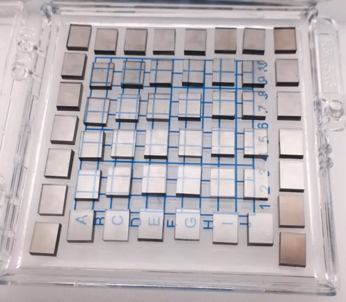
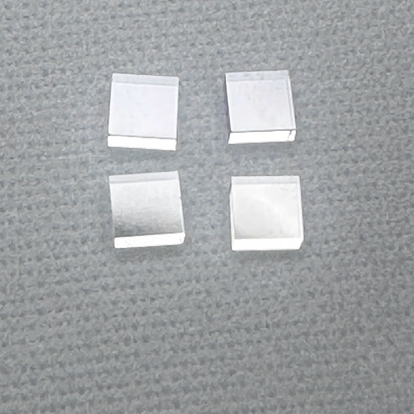
Lab-grown single-crystal diamond wafers are ultra-high-performance substrates produced by Chemical Vapor Deposition (CVD), offering unmatched thermal conductivity, hardness, optical transparency, and crystal purity. Unlike polycrystalline diamond, single-crystal diamond provides a uniform lattice structure with minimal grain boundaries, making it ideal for advanced electronics, photonics, quantum devices, and precision optics.
Our diamond wafers are carefully grown, cut, and polished to deliver research-grade surface quality and controlled crystallographic orientation. They are widely used as heat spreaders for high-power devices, substrates for GaN/AlN/diamond electronics, quantum NV-center platforms, and optical or X-ray components requiring extreme durability.
Key Features
- True single-crystal CVD diamond
- Exceptional thermal conductivity (up to ~2000 W/m·K)
- Ultra-low impurity & defect density
- Atomically smooth polished surface
- Controlled crystal orientation: {100}, {110}, or custom
- Custom cutting, thickness, and polishing available
Typical Specifications
- Material: Single-crystal CVD diamond
- Form: Wafer / plate / substrate
- Orientation: {100} (standard), others on request
- Thickness: 0.1 – 0.6 mm (custom available)
- Surface Finish: Optical polish (Ra < 30–50 nm typical) Ra ~1nm available for request
- Size: mm-scale to cm-scale (custom sizes supported)
Applications
- High-power semiconductor heat spreaders
- Diamond-based electronics & RF devices
- Quantum computing (NV centers)
- MEMS / NEMS fabrication
- X-ray, laser, and infrared optics
- Extreme-environment research
Frequently Asked Questions — Single-Crystal Diamond Wafer
What is a lab-grown single-crystal diamond wafer?
How does single-crystal diamond differ from polycrystalline diamond?
What crystal orientations are available?
What surface finish and thickness can you provide?
What are common applications of diamond wafers?
Are these wafers suitable for semiconductor processing?
Do you offer custom sizes, shapes, or edge processing?
Are these wafers suitable for research and OEM use?
📘 Related Knowledge
Share