My Store
Custom Sapphire Wafers & Substrates for Epitaxy
Custom Sapphire Wafers & Substrates for Epitaxy
Couldn't load pickup availability
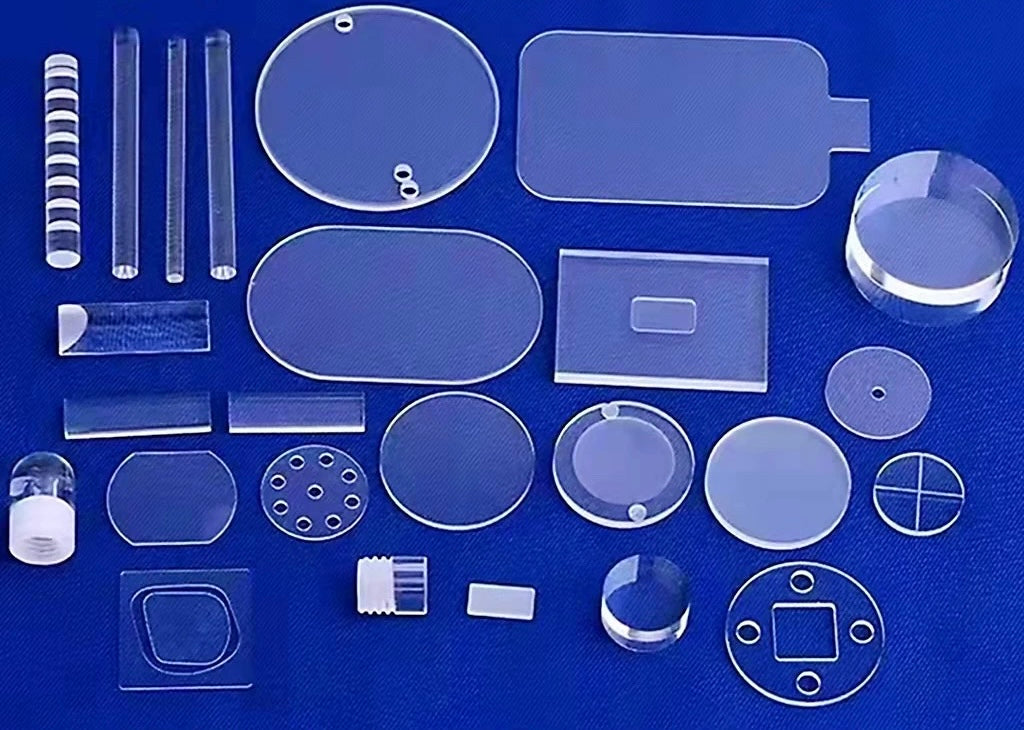
Sapphire wafers and substrates are high-quality single crystal materials composed of aluminum oxide (Al₂O₃), widely used in semiconductor epitaxy, LED manufacturing, RF devices, power electronics, and optical applications. Sapphire combines exceptional mechanical strength, thermal stability, chemical inertness, and excellent optical transparency, making it one of the most versatile substrate materials in advanced technology fields.
With a wide optical transmission range from the ultraviolet to mid-infrared, sapphire substrates are well suited for optoelectronic and photonic devices. At the same time, their high melting point and thermal conductivity enable stable operation during high-temperature epitaxial growth processes such as MOCVD, MBE, and HVPE.
Sapphire wafers are most commonly used as substrates for GaN-based epitaxy, supporting the fabrication of LEDs, laser diodes, RF amplifiers, and power devices. Multiple crystallographic orientations are available to optimize lattice matching, surface morphology, and device performance for specific material systems.
Our sapphire substrates are manufactured with strict control of crystal orientation, surface flatness, thickness uniformity, and defect density. Precision polishing ensures low surface roughness suitable for epitaxial growth and microfabrication, supporting both research-scale development and commercial production.
Key Features & Properties
- Material: Single crystal sapphire (Al₂O₃)
- Excellent mechanical strength and hardness
- High thermal stability and high melting point
- Wide optical transmission range (UV–IR)
- Chemically inert and corrosion resistant
- Low surface roughness and high flatness
- Compatible with high-temperature epitaxy
Typical Applications
- GaN-based LED and laser diode substrates
- RF and microwave devices
- Power electronics and high-temperature devices
- Semiconductor epitaxial growth
- Optical windows and substrates
- Sensors and MEMS devices
Custom wafer sizes, thicknesses, orientations, and surface finishes are available upon request.
Properties:
- Material: High Purity >99.99%, single crystal Al2O3
- Thickness: 430 um +/- 25 um for SSP and 400 um +/- 15 um for DSP (other thickness available upon request)
- Orientation: C plane (0001) to M (1-100) 0.2 +/- 0.1 degree off.
- Polishing: single side polished polished side surface Ra < 0.3 nm, back side fine-ground Ra = 0.8 ~ 1.2 um, or double side polished both front and back sides surface Ra < 0.3 nm
- Minimum Order Quantity (MOQ): 10 pieces per order
Frequently Asked Questions — Sapphire Wafers & Substrates
What are sapphire wafers used for?
Why is sapphire commonly used for GaN epitaxy?
What crystal orientations are available?
What surface finish options are offered?
Are sapphire wafers compatible with high-temperature processing?
What wafer sizes and thicknesses are available?
Are sapphire substrates suitable for both research and mass production?
Can you provide custom specifications?
📘 Related Knowledge
Share