My Store
Single-Crystal GaN Wafers for Power & RF Electronics
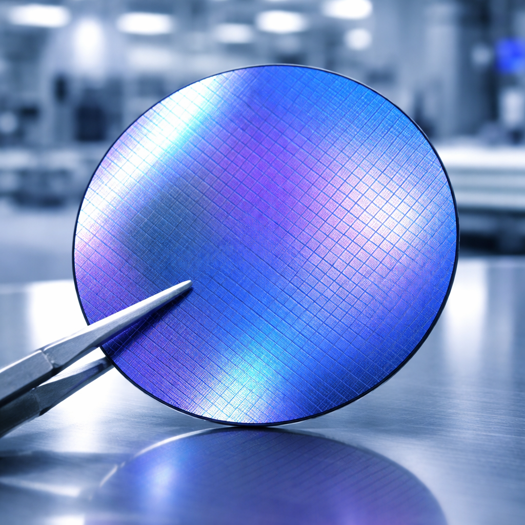
Single-Crystal GaN Wafers for Power & RF Electronics
Couldn't load pickup availability
GaN (Gallium Nitride) substrates and wafers are high-performance semiconductor materials widely used in power electronics, RF and microwave devices, LEDs, laser diodes, and advanced optoelectronic systems. As a wide-bandgap semiconductor with a bandgap of approximately 3.4 eV, GaN enables devices with high breakdown voltage, high electron mobility, high switching speed, and excellent thermal stability.
Compared with hetero-epitaxial GaN grown on sapphire or silicon, native GaN substrates offer significantly lower dislocation density, improved crystal quality, and superior device reliability. These advantages are critical for high-power, high-frequency, and high-efficiency devices, including GaN HEMTs, vertical power devices, and high-brightness laser diodes.
GaN wafers provide excellent lattice matching for homoepitaxial growth, enabling precise control of epitaxial layers and device structures. This results in higher yield, improved performance uniformity, and longer device lifetime, making GaN substrates the material of choice for next-generation semiconductor technologies.
Our GaN substrates are supplied with strict control of orientation, surface flatness, thickness uniformity, and defect density. Precision polishing ensures ultra-smooth surfaces suitable for MOCVD, MBE, and HVPE epitaxy. Multiple orientations, doping types, and wafer sizes are available to support both academic research and commercial device manufacturing.
Key Features & Properties
- Material: Single crystal Gallium Nitride (GaN)
- Wide bandgap: ~3.4 eV
- High breakdown electric field
- High electron mobility and saturation velocity
- Low dislocation density (native GaN)
- Excellent thermal and chemical stability
- Optimized for homoepitaxial growth
Typical Applications
- Power electronics and vertical GaN devices
- RF and microwave HEMTs
- High-brightness LEDs
- Blue and UV laser diodes
- High-frequency and high-efficiency electronics
- Advanced optoelectronic and photonic devices
Custom wafer sizes, orientations, surface finishes, and doping options are available upon request.
Frequently Asked Questions — GaN Substrates & Wafers
What is a GaN substrate or wafer?
Why choose native GaN instead of GaN-on-sapphire or GaN-on-Si?
What applications benefit most from GaN substrates?
What epitaxy techniques are compatible with GaN wafers?
What crystal orientations are available?
What surface quality and polishing are provided?
Are different doping types available?
What wafer sizes are supported?
Are GaN substrates suitable for research and mass production?
Can custom specifications be supported?
Share